BOSMAL a certified supplier of further laboratory services for the Volkswagen Group
Scanning electron microscopy (SEM)
Scanning electron microscope with the ability to work in various vacuum modes, which allows analysis of both conductive and nonconductive samples. It has the ability to image SE (secondary electron) and BSE (backscattered electron), it is also equipped with EDS (energy dispersive X-ray spectroscopy) Oxford analyzer and EBSD (electron backscatter diffraction) Bruker analyzer.
Research capacity:
- Qualitative and quantitative analysis and mapping of elemental composition of samples.
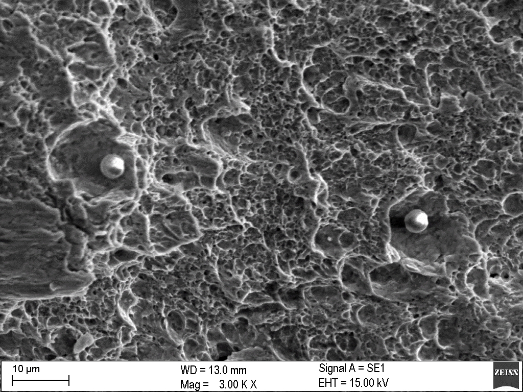
- Evaluation of fractography of the fracture surface to determine the nature of the crack, material discontinuities and, for example, hydrogen embrittlement.
- Analysis of the size and type of non-metallic inclusions.
- Linear microanalysis of coatings and diffusion layers.
- Classification of pollutants on the filters - technical cleanliness tests.
- Possibility to test samples with larger dimensions (300x200x200 mm) due to the large chamber.
Apparatus
- SEM EVO MA25 scanning electron microscope with Oxford Instruments EDS analyzer and Bruker EBSD analyzer
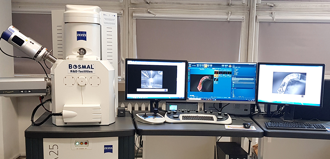

View of an object under the SEM microscope

Elemental composition